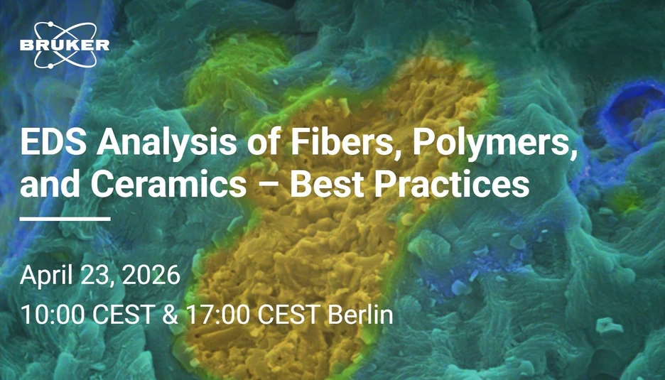
EDS Analysis of Fibers, Polymers, and Ceramics – Best Practices
Join us for a concise 40-minute session, where Bruker's experts guide you through the different EDS measurement approaches using conventional geometry and an annular approach (QUANTAX FlatQUAD) making the best choice for challenging analytical tasks.
In this webinar we will:
- Present and compare EDS results with different measurement setups on various challenging samples with technological relevance (nonconductive and/or beam sensitive materials).
- Review sample preparation strategies and how they affect the EDS measurements.
Finding optimal measurement setup for energy dispersive spectroscopy (EDS) and conditions for a given analytical task can be a complex matter. The common requirements for SEM-EDS analysis, such as “the sample has to be flat/polished and electrically conductive” cannot be met all times. In many cases, samples have to be analyzed under native or as-received conditions, and the microscopist must find the right setup and conditions to provide answers in the shortest possible time.
The optimal analytical setup is a combination of the right choice of EDS detector, sample preparation options, SEM imaging/measurement and vacuum conditions.
This webinar will present a comparative approach to demonstrate which combination of these parameters provides best conditions to answer the current analytical question.
Among others we will compare optimized results and how to achieve these on the following samples with:
- No or low electrical conductivity (building materials and polymers with fracture test surfaces).
- Rough surface morphology (fibers on filter with particles to detect).
- High beam sensitivity (“soft” materials and life science samples).
Who should attend?
- Industry professionals wanting to use EDS as a fast and accurate material characterization method.
- Electron Microscopists dealing with complex samples and analytical tasks.
- Anyone interested in elemental analysis for materials science, life science, building materials and polymers.
Speaker: Dr. Igor Németh (Application Scientist EDS, Bruker Nano Analytics)
Speaker: Dr. Purvesh Soni (Sr. Applications Scientist EDS, Bruker Electron Microscope Analyzers)