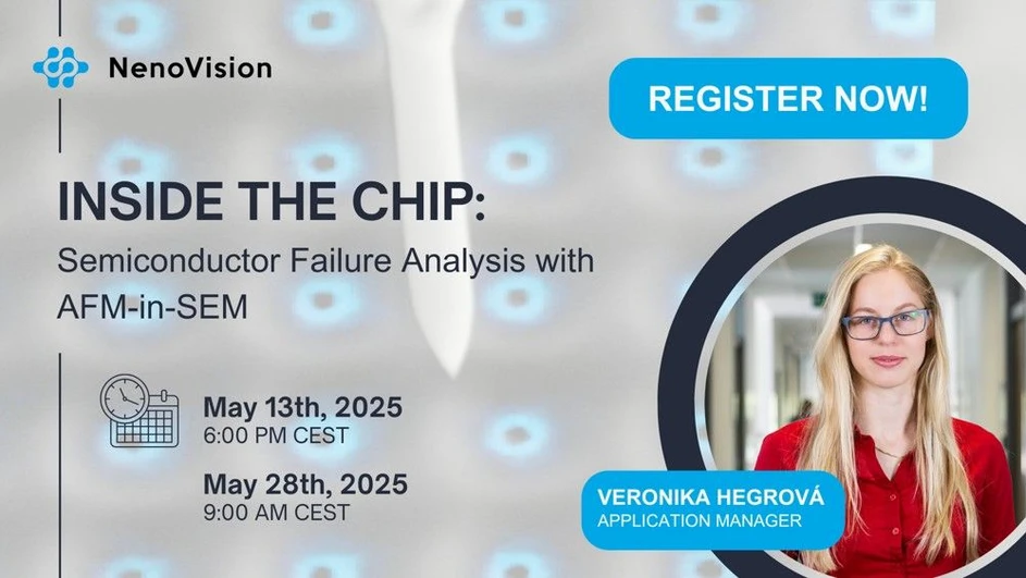
Inside the Chip: Semiconductor Failure Analysis with AFM-in-SEM
Dive into the world of semiconductor failure analysis and discover how integrated AFM-in-SEM technology enables in-situ, high-resolution electrical and topographical characterization - right where it matters most.
Learn how LiteScope transforms traditional workflows by combining SEM, FIB, and AFM techniques into a single, efficient process - streamlining diagnostics and revealing the root causes of device failure with nanoscale precision.
This webinar will walk you through real application examples, including dopant profiling of MOSFET transistors and conductivity mapping of complex semiconductor structures.
We’re running this webinar twice for our global audience - pick whichever timeslot fits your schedule the best!
Session 2 - May 28, 09:00 CEST - REGISTER HERE
Session 1 - May 13, 18:00 CEST - REGISTER HERE
In this webinar, you will learn how to:
- Navigate directly to specific vias, transistors, or doped layers and perform localized electrical characterization.
- Eliminate sample transfers with an integrated SEM, FIB, and AFM in-situ workflow.
- Streamline diagnostics of device failures at the nanoscale level to speed up your R&D process.
- Use LiteScope in real-world cases like dopant profiling of MOSFET transistors and conductivity mapping of complex semiconductor structures.
Presenter: Veronika Hegrová (Application manager, NenoVision s.r.o.)